07 Serial Peripheral Interface(SPI)
원문 : http://kkamagui.springnote.com/pages/422905
들어가기 전에...
- 이 글은 kkamagui에 의해 작성된 글입니다.
- 마음껏 인용하시거나 사용하셔도 됩니다. 단 출처(http://kkamagui.tistory.com, http://kkamagui.springnote.com)는 밝혀 주십시오.
- 기타 사항은 mint64os at gmail.com 이나 http://kkamagui.tistory.com으로 보내주시면 반영하겠습니다.
- OS 제작에 대한 상세한 내용은 책 "64비트 멀티코어 OS 구조와 원리"를 참고하기 바랍니다.
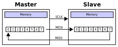
Serial Pheripheral Interface(SPI)는 FULL Duplex로 동작하는 Mototola에서 개발된 버스이다. 자세한 내용은 wikipedia http://en.wikipedia.org/wiki/Serial_peripheral_interface에서 찾을 수 있으며 하나의 Master와 하나 이상의 Slave의 컨트롤러로 이루어진다.
1.구성 및 설명
<Master-Slave SPI>
좌측과 같이 Master/Slave가 1:1로 연결될 수 있고, 우측과 같이 1:n으로 연결하는 것도 가능하다. NDS의 SPI 컨트롤에서 Chip Select가 있는 것을 보아 다수의 컨트롤러가 묶여있는 것 같다.
Interface
The SPI bus specifies four logic signals.
- SCLK — Serial Clock (output from master)
- MOSI/SIMO — Master Output, Slave Input (output from master)
- MISO/SOMI — Master Input, Slave Output (output from slave)
- SS — Slave Select (active low; output from master)
Alternative naming conventions are also widely used:
- SCK — Serial Clock (output from master)
- SDI, DI, SI — Serial Data In
- SDO, DO, SO — Serial Data Out
- nCS, CS, nSS, STE — Chip Select, Slave Transmit Enable (active low; output from master)
The SDI/SDO (DI/DO, SI/SO) convention requires that SDO on the master be connected to SDI on the slave, and vice-versa. That's confusing, so the MOSI/MISO convention is preferred.
- SPI port pin names for particular IC products may differ from those depicted in these illustrations.
2.동작방법
The SPI bus can operate with a single master device and with one or more slave devices.
If a single slave device is used, the SS pin may be fixed to logic low if the slave permits it. Some slaves require the falling edge (high->low transition) of the slave select to initiate an action such as the MAX1242 by Maxim IC, an ADC, that starts conversion on said transition. With multiple slave devices, an independent SS signal is required from the master for each slave device.Most devices have tri-state outputs that become high impedance ("disconnected") when the device is not selected. Devices without tristate outputs can't share SPI bus segments with other devices; only one such slave may talk to the master, and only its chipselect may be activated.
Data Transmission
To begin a communication, the master first configures the clock, using a frequency less than or equal to the maximum frequency the slave device supports. Such frequencies are commonly in the range of 1-70 MHz.
The master then pulls the slave select low for the desired chip. If a waiting period is required (such as for analog-to-digital conversion) then the master must wait for at least that period of time before starting to issue clock cycles.
During each SPI clock cycle, a full duplex data transmission occurs:
- the master sends a bit on the MOSI line; the slave reads it from that same line
- the slave sends a bit on the MISO line; the master reads it from that same line
Not all transmissions require all four of these operations to be meaningful but they do happen.
The transmissions normally involve two shift registers of some given word size, such as eight bits, one in the master and one in the slave; they are connected in a ring. Data is usually shifted out with the most significant bit first, while shifting a new least significant bit into the same register. After that register has been shifted out, the master and slave have exchanged register values. Then each device takes that value and does something with it, such as writing it to memory. If there is more data to exchange, the shift registers are loaded with new data and the process repeats.
Transmissions may involve any number of clock cycles. When there are no more data to be transmitted, the master stops toggling its clock. Normally, it then deselects the slave.
Transmissions often use single 8-bit bytes, and a master can initiate multiple such transmissions if it wishes/needs. However, other word sizes are also common, such as 16-bit words for touchscreen controllers or audio codecs, like the TSC2101 from Texas Instruments; or 12-bit words for many digital-to-analog or analog-to-digital converters.
Every slave on the bus that hasn't been activated using its slave select line must disregard the input clock and MOSI signals, and may not drive MISO. The master selects only one slave at a time.

3.인터럽트(Interrupt)
Interrupts
SPI devices sometimes use another signal line to send an interrupt signal to a host CPU. Examples include pen-down interrupts from touchscreen sensors, thermal limit alerts from temperature sensors, alarms issued by real time clock chips, and headset jack insertions from the sound codec in a cell phone.
위에서 NDS의 Pen Down 예제를 들어서 설명해 놓은 것이 있다.
4.NDS의 SPI
4.1 SPI 레지스터
NDS에 연결되어있는 SPI의 구성은 http://nocash.emubase.de/gbatek.htm#dsserialperipheralinterfacebusspi 에서 찾아볼 수 있다.
Serial Peripheral Interface Bus
SPI Bus is a 4-wire (Data In, Data Out, Clock, and Chipselect) serial bus.
The NDS supports the following SPI devices (each with its own chipselect).
DS Firmware Serial Flash Memory
DS Touch Screen Controller (TSC)
DS Power Management
40001C0h - SPICNT - NDS7 - SPI Bus Control/Status RegisterThe "Hold" flag should be cleared BEFORE transferring the LAST data unit, the chipselect will be then automatically cleared after the transfer, the program should issue a WaitByLoop(3) manually AFTER the LAST transfer.
SPI Control 레지스터를 설정할 때 주의할 점은 마지막 Command or Data를 송신할때는 Chipselect Hold를 미리 0으로 설정해 놓아야 한다는 것이다. 이것을 하지 않으면 Chipselect가 자동으로 해제되지 않으므로 해당 칩을 계속 물고 있게 된다.
- 1Byte의 명령만 송신할 때 : chipselect를 0으로 설정해서 명령을 송신한 다음 데이터를 수신받음
- 2Byte 이상의 명령 + 데이터의 형태를 송신할 때 : chipselect를 1로 설정하여 데이터를 송신한 다음 마지막 바이트에서는 chipselect를 0으로 한다음 송신
40001C2h - SPIDATA - NDS7 - SPI Bus Data/Strobe Register (R/W)
The SPI transfer is started on writing to this register, so one must <write> a dummy value (should be zero) even when intending to <read> from SPI bus.
During transfer, the Busy flag in SPICNT is set, and the written SPIDATA value is transferred to the device (via output line), simultaneously data is received (via input line). Upon transfer completion, the Busy flag goes off (with optional IRQ), and the received value can be then read from SPIDATA, if desired.
데이터를 송/수신 할때 주의할 점은 SPI Control 레지스터의 Busy bit가 0일때 보내야 한다는 것이다. Busy bit가 1일때는 데이터를 송신 중이거나 수신중이기 때문에 보내거나 받으면 안된다.
Notes/Glitches
SPICNT Bits 12,13 appear to be unused (always zero), although the BIOS (attempts to) set Bit13=1, and Bit12=Bit11 when accessing the firmware.
The SPIDATA register is restricted to 8bit, so that only each second byte will appear in the register when attemting to use the bugged 16bit mode.
Cartridge Backup Auxiliar SPI Bus
The NDS Cartridge Slot uses a separate SPI bus (with other I/O Ports), see
DS Cartridge Backup
위는 참고적인 사항이니 그냥 넘어가자.
4.2 SPI 사용 순서
4.2.1 명령 송신
SPI를 통해 해당 Device로 명령과 데이터를 송신할때 아래와 같은 순서로 하면 된다.
- Busy 상태인가 확인 후 NON BUSY 상태 체크
- SPI Control 레지스터에 SPI 사용 가능 및 클럭, Continous 모드 설정
- SPI Data 레지스터에 명령 or 데이터 송신
- Busy 상태인가 확인후 NON BUSY 상태 체크
- 3~4를 마지막 데이터 or 명령까지 반복. 마지막 데이터의 경우 SPI Control 레지스터에 Continous 모드를 제거하고 송신
4.2.2 데이터 수신
SPI를 통한 데이터 수신의 경우에는 명령을 보내고 수신 요청(0x00을 SPI Data 레지스터에 씀)을 함으로써 바로 받을 수 있다.
- Busy 상태인가 확인 후 NON BUSY 상태 체크
- SPI Control 레지스터에 SPI 사용 가능 및 클럭, Continous 모드 설정
- SPI Data 레지스터에 명령 or 데이터 송신
- Busy 상태인가 확인후 NON BUSY 상태 체크
- SPI Data 레지스터에 0x00 패킷 송신
- Busy 상태인가 확인후 NON BUSY 상태 체크
- SPI Data 레지스터에서 값을 읽음
- 4~7을 마지막 데이터까지 반복. 마지막 데이터의 경우 SPI Control 레지스터에 Continous 모드를 제거하고 Dummy Data 송신
5.구현
SPI는 ARM7에만 있으므로 \devkitPro\libnds\srouce\include\nds\arm7 폴더에서 serial.h 파일을 찾아야 한다.
// SPI chain registers
#define REG_SPICNT (*(vuint16*)0x040001C0)
#define REG_SPIDATA (*(vuint16*)0x040001C2)#define SPI_ENABLE BIT(15)
#define SPI_IRQ BIT(14)
#define SPI_BUSY BIT(7)
// Pick the SPI clock speed
#define SPI_BAUD_4MHZ 0
#define SPI_BAUD_2MHZ 1
#define SPI_BAUD_1MHZ 2
#define SPI_BAUD_512KHZ 3
// meh
#define SPI_BAUD_4MHz 0
#define SPI_BAUD_2MHz 1
#define SPI_BAUD_1MHz 2
#define SPI_BAUD_512KHz 3
// Pick the SPI transfer length
#define SPI_BYTE_MODE (0<<10)
#define SPI_HWORD_MODE (1<<10)
// Pick the SPI device
#define SPI_DEVICE_POWER (0 << 8)
#define SPI_DEVICE_FIRMWARE (1 << 8)
#define SPI_DEVICE_NVRAM (1 << 8)
#define SPI_DEVICE_TOUCH (2 << 8)
#define SPI_DEVICE_MICROPHONE (2 << 8)
// When used, the /CS line will stay low after the transfer ends
// i.e. when we're part of a continuous transfer
#define SPI_CONTINUOUS BIT(11)
위에서 설명했던 각 Register의 값과 비트를 설정해 놓았다는 것을 알 수 있다.
이 헤더 파일을 사용해서 직접 Power Control을 한 예제를 보자. \devkitPro\libnds\source\source\arm7 폴더에서 spi.c 파일을 찾으면 된다.
- //---------------------------------------------------------------------------------
int writePowerManagement(int reg, int command) {
//---------------------------------------------------------------------------------
// Write the register / access mode (bit 7 sets access mode) - while (REG_SPICNT & SPI_BUSY);
REG_SPICNT = SPI_ENABLE | SPI_BAUD_1MHZ | SPI_BYTE_MODE | SPI_CONTINUOUS | SPI_DEVICE_POWER;
REG_SPIDATA = reg; - // Write the command / start a read
while (REG_SPICNT & SPI_BUSY);
REG_SPICNT = SPI_ENABLE | SPI_BAUD_1MHZ | SPI_BYTE_MODE | SPI_DEVICE_POWER;
REG_SPIDATA = command; - // Read the result
while (REG_SPICNT & SPI_BUSY);
return REG_SPIDATA & 0xFF;
}
위에서 보면 2Byte의 Command를 날려야 하는데, 첫번째 송신때는 SPI_CONTINUOUS를 사용했지만 두번째는 SPI_CONTINOUS를 사용하지 않은 것을 알 수 있다.
6.마치면서...
SPI의 동작 및 NDS에 적용된 부분을 살펴보았다. 이제 ARM7 코드만 손보면 우리가 원하는 작업을 할 수 있게 되었다. Power Control 같은 경우도 Memory Map Register를 사용해서 할 수 없었던 부분을 할 수 있다.
이것 저것 많이 테스트 해보도록 하자 >ㅁ<)/~
이 글은 스프링노트에서 작성되었습니다.
'NDS 홈브루(Homebrew) > 홈브루 Tutorial' 카테고리의 다른 글
| 08 사운드(Sound) 제어 (0) | 2007.11.14 |
|---|---|
| 07 문쉘(Moon shell)의 터치스크린(Touch Screen) 소스 (0) | 2007.11.14 |
| 06 키패드(KeyPad) 및 터치스크린(Touch Screen) 제어 (0) | 2007.11.14 |
| 05 파워 컨트롤(Power Control) (0) | 2007.11.14 |
| 04 인터럽트 제어(Interrupt Control) (0) | 2007.11.14 |